- 您现在的位置:买卖IC网 > Sheet目录2003 > LTC1403AIMSE-1#TRPBF (Linear Technology)IC ADC 14BIT 2.8MSPS DIFF 10MSOP
LTC1403-1/LTC1403A-1
4
14031fc
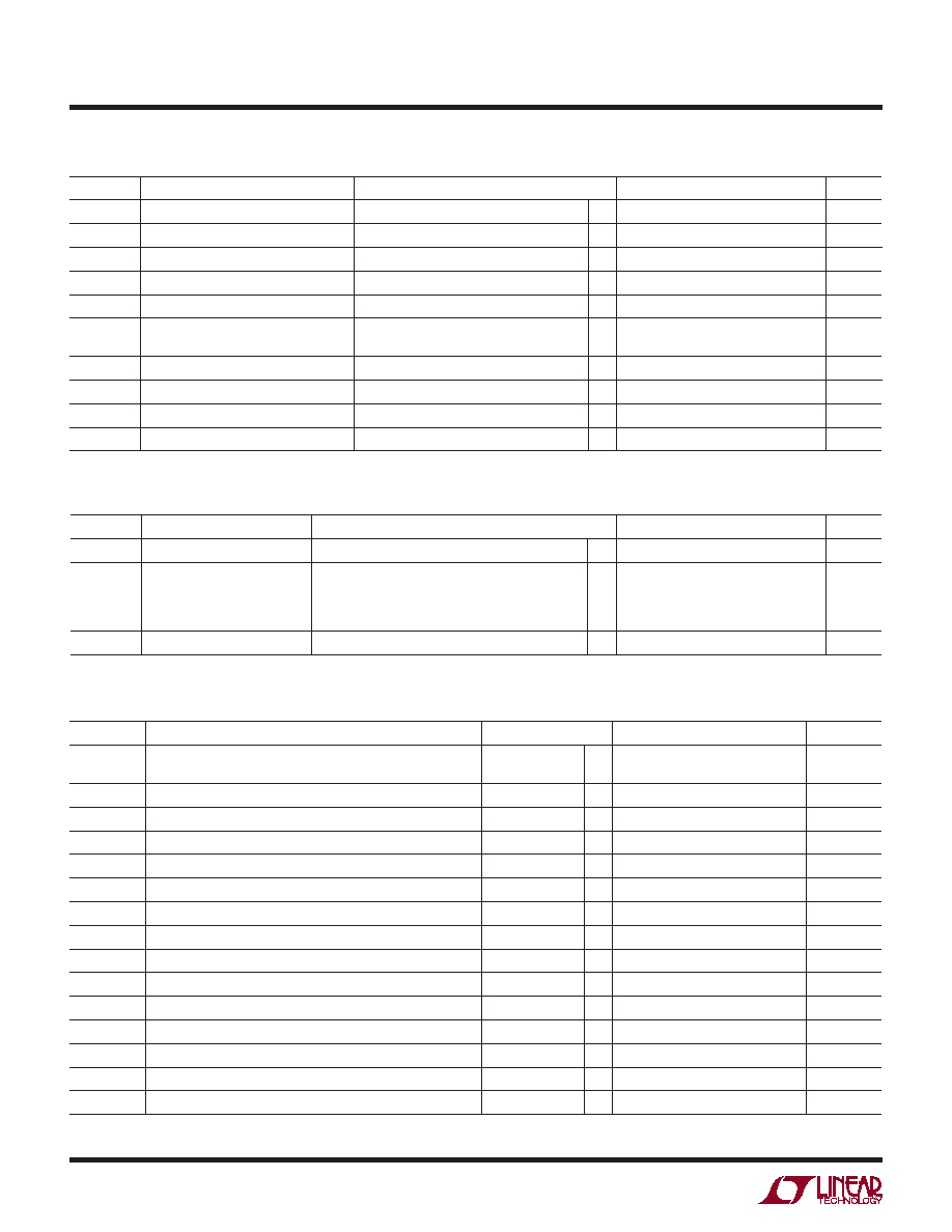
TIMING CHARACTERISTICS
DIGITAL INPUTS AND DIGITAL OUTPUTS
SYMBOL
PARAMETER
CONDITIONS
MIN
TYP
MAX
UNITS
VIH
High Level Input Voltage
VDD = 3.3V
l
2.4
V
VIL
Low Level Input Voltage
VDD = 2.7V
l
0.6
V
IIN
Digital Input Current
VIN = 0V to VDD
l
±10
A
CIN
Digital Input Capacitance
(Note 20)
5
pF
VOH
High Level Output Voltage
VDD = 3V, IOUT = –200A
l
2.5
2.9
V
VOL
Low Level Output Voltage
VDD = 2.7V, IOUT = 160A
VDD = 2.7V, IOUT = 1.6mA
l
0.05
0.10
0.4
V
IOZ
Hi-Z Output Leakage DOUT
VOUT = 0V to VDD
l
±10
A
COZ
Hi-Z Output Capacitance DOUT
1
pF
ISOURCE
Output Short-Circuit Source Current
VOUT = 0V, VDD = 3V
20
mA
ISINK
Output Short-Circuit Sink Current
VOUT = VDD = 3V
15
mA
POWER REQUIREMENTS The
l
denotes the specifications which apply over the full operating temperature
range, otherwise specifications are at TA = 25°C. (Note 17)
SYMBOL
PARAMETER
CONDITIONS
MIN
TYP
MAX
UNITS
VDD
Supply Voltage
2.7
3.6
V
IDD
Positive Supply Voltage
Active Mode
Nap Mode
Sleep Mode (LTC1403-1)
Sleep Mode (LTC1403A-1)
l
4.7
1.1
2
7
1.5
15
10
mA
A
PD
Power Dissipation
Active Mode with SCK in Fixed State (Hi or Lo)
12
mW
The l denotes the specifications which apply over the full operating temperature
range, otherwise specifications are at TA = 25°C. VDD = 3V
SYMBOL
PARAMETER
CONDITIONS
MIN
TYP
MAX
UNITS
fSAMPLE(MAX) Maximum Sampling Frequency per Channel
(Conversion Rate)
l
2.8
MHz
tTHROUGHPUT Minimum Sampling Period (Conversion + Acquisition Period)
l
357
ns
tSCK
Clock Period
(Note 16)
l
19.8
10000
ns
tCONV
Conversion Time
(Note 6)
16
18
SCLK cycles
t1
Minimum Positive or Negative SCLK Pulse Width
(Note 6)
2
ns
t2
CONV to SCK Setup Time
(Notes 6, 10)
3
ns
t3
Nearest SCK Edge Before CONV
(Note 6)
0
ns
t4
Minimum Positive or Negative CONV Pulse Width
(Note 6)
4
ns
t5
SCK to Sample Mode
(Note 6)
4
ns
t6
CONV to Hold Mode
(Notes 6, 11)
1.2
ns
t7
16th SCK↑ to CONV↑ Interval (Affects Acquisition Period)
(Notes 6, 7, 13)
45
ns
t8
Minimum Delay from SCKto Valid Data
(Notes 6, 12)
8
ns
t9
SCK to Hi-Z at SDO
(Notes 6, 12)
6
ns
t10
Previous SDO Bit Remains Valid After SCK
(Notes 6, 12)
2
ns
t12
VREF Settling Time After Sleep-to-Wake Transition
(Notes 6, 14)
2
ms
The l denotes the specifications which apply over the
full operating temperature range, otherwise specifications are at TA = 25°C. VDD = 3V
发布紧急采购,3分钟左右您将得到回复。
相关PDF资料
LTC1404IS8#TRPBF
IC A/D CONV 12BIT W/SHTDN 8-SOIC
LTC1405IGN#TRPBF
IC ADC 12BIT 5MSPS SAMPLE 28SSOP
LTC1406IGN#TRPBF
IC A/D CONV 8BIT SAMPLING 24SSOP
LTC1407AHMSE#PBF
IC ADC 14BIT 3MSPS 10-MSOP
LTC1407AIMSE-1#TRPBF
IC ADC 14BIT 3MSPS SAMPLE 10MSOP
LTC1408IUH-12#TRPBF
IC ADC 12BIT 600KSPS 32-QFN
LTC1408IUH#TRPBF
IC ADC 14BIT 600KSPS 32-QFN
LTC1409IG#TR
IC ADC 12BIT 800KSPS SMPL 28SSOP
相关代理商/技术参数
LTC1403CMSE
功能描述:IC ADC 12BIT 2.8MSPS DIFF 10MSOP RoHS:否 类别:集成电路 (IC) >> 数据采集 - 模数转换器 系列:- 标准包装:1,000 系列:- 位数:16 采样率(每秒):45k 数据接口:串行 转换器数目:2 功率耗散(最大):315mW 电压电源:模拟和数字 工作温度:0°C ~ 70°C 安装类型:表面贴装 封装/外壳:28-SOIC(0.295",7.50mm 宽) 供应商设备封装:28-SOIC W 包装:带卷 (TR) 输入数目和类型:2 个单端,单极
LTC1403CMSE#PBF
功能描述:IC ADC 12BIT 2.8MSPS 10-MSOP RoHS:是 类别:集成电路 (IC) >> 数据采集 - 模数转换器 系列:- 标准包装:1 系列:microPOWER™ 位数:8 采样率(每秒):1M 数据接口:串行,SPI? 转换器数目:1 功率耗散(最大):- 电压电源:模拟和数字 工作温度:-40°C ~ 125°C 安装类型:表面贴装 封装/外壳:24-VFQFN 裸露焊盘 供应商设备封装:24-VQFN 裸露焊盘(4x4) 包装:Digi-Reel® 输入数目和类型:8 个单端,单极 产品目录页面:892 (CN2011-ZH PDF) 其它名称:296-25851-6
LTC1403CMSE#TR
功能描述:IC ADC 12BIT 2.8MSPS DIFF 10MSOP RoHS:否 类别:集成电路 (IC) >> 数据采集 - 模数转换器 系列:- 标准包装:1,000 系列:- 位数:16 采样率(每秒):45k 数据接口:串行 转换器数目:2 功率耗散(最大):315mW 电压电源:模拟和数字 工作温度:0°C ~ 70°C 安装类型:表面贴装 封装/外壳:28-SOIC(0.295",7.50mm 宽) 供应商设备封装:28-SOIC W 包装:带卷 (TR) 输入数目和类型:2 个单端,单极
LTC1403CMSE#TRPBF
功能描述:IC ADC 12BIT 2.8MSPS DIFF 10MSOP RoHS:是 类别:集成电路 (IC) >> 数据采集 - 模数转换器 系列:- 标准包装:1,000 系列:- 位数:16 采样率(每秒):45k 数据接口:串行 转换器数目:2 功率耗散(最大):315mW 电压电源:模拟和数字 工作温度:0°C ~ 70°C 安装类型:表面贴装 封装/外壳:28-SOIC(0.295",7.50mm 宽) 供应商设备封装:28-SOIC W 包装:带卷 (TR) 输入数目和类型:2 个单端,单极
LTC1403CMSE-1
功能描述:IC ADC 12BIT 2.8MSPS DIFF 10MSOP RoHS:否 类别:集成电路 (IC) >> 数据采集 - 模数转换器 系列:- 标准包装:1,000 系列:- 位数:16 采样率(每秒):45k 数据接口:串行 转换器数目:2 功率耗散(最大):315mW 电压电源:模拟和数字 工作温度:0°C ~ 70°C 安装类型:表面贴装 封装/外壳:28-SOIC(0.295",7.50mm 宽) 供应商设备封装:28-SOIC W 包装:带卷 (TR) 输入数目和类型:2 个单端,单极
LTC1403CMSE-1#PBF
功能描述:IC ADC 12BIT 2.8MSPS 10-MSOP RoHS:是 类别:集成电路 (IC) >> 数据采集 - 模数转换器 系列:- 标准包装:1 系列:microPOWER™ 位数:8 采样率(每秒):1M 数据接口:串行,SPI? 转换器数目:1 功率耗散(最大):- 电压电源:模拟和数字 工作温度:-40°C ~ 125°C 安装类型:表面贴装 封装/外壳:24-VFQFN 裸露焊盘 供应商设备封装:24-VQFN 裸露焊盘(4x4) 包装:Digi-Reel® 输入数目和类型:8 个单端,单极 产品目录页面:892 (CN2011-ZH PDF) 其它名称:296-25851-6
LTC1403CMSE-1#TR
功能描述:IC ADC 12BIT 2.8MSPS DIFF 10MSOP RoHS:否 类别:集成电路 (IC) >> 数据采集 - 模数转换器 系列:- 标准包装:1,000 系列:- 位数:16 采样率(每秒):45k 数据接口:串行 转换器数目:2 功率耗散(最大):315mW 电压电源:模拟和数字 工作温度:0°C ~ 70°C 安装类型:表面贴装 封装/外壳:28-SOIC(0.295",7.50mm 宽) 供应商设备封装:28-SOIC W 包装:带卷 (TR) 输入数目和类型:2 个单端,单极
LTC1403CMSE-1#TRPBF
功能描述:IC ADC 12BIT 2.8MSPS DIFF 10MSOP RoHS:是 类别:集成电路 (IC) >> 数据采集 - 模数转换器 系列:- 标准包装:1,000 系列:- 位数:16 采样率(每秒):45k 数据接口:串行 转换器数目:2 功率耗散(最大):315mW 电压电源:模拟和数字 工作温度:0°C ~ 70°C 安装类型:表面贴装 封装/外壳:28-SOIC(0.295",7.50mm 宽) 供应商设备封装:28-SOIC W 包装:带卷 (TR) 输入数目和类型:2 个单端,单极